RF - Resonant Circuit - Load Q Value 🚧
The Q value of a resonant circuit, also known as the load Q value, is defined as the ratio of the center frequency to the 3dB bandwidth of the resonant circuit. It describes the passband characteristics of the resonant circuit under actual circuit or load conditions. The load Q of a resonant circuit depends on three main factors:
- Source impedance \(R_s\)
- Load resistance \(R_L\)
- Q value of the components mentioned in the previous chapter
Influence of \(R_s\) and \(R_L\) on Load Q
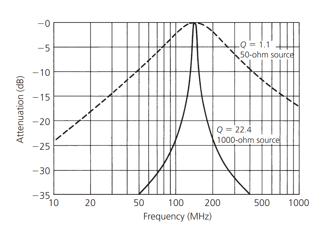
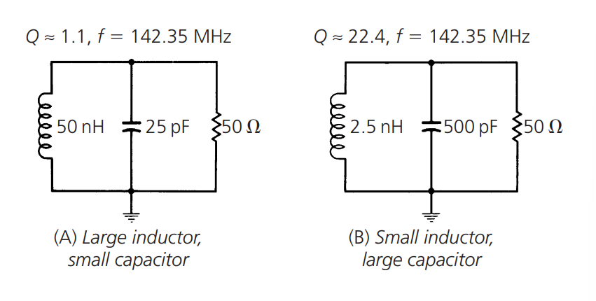
The influence of source impedance and load impedance on the load Q of a resonant circuit is shown in the above figure. The original curve (dashed line) represents the resonance curve of a circuit consisting of a 50Ω source impedance, a lossless inductor of 0.05uH, and a lossless capacitor of 25pF. The Q value, calculated using the formula \(Q=\frac{f_e}{f_2-f_1}\) mentioned earlier, is approximately 1.1. Obviously, this is not a very narrowband or high Q value design.
By changing the source impedance to 1000Ω, a new resonance curve (solid line) is plotted, and the Q value of the resonant circuit increases significantly to 22.4. By increasing the source impedance, we increase the Q value of the resonant circuit.
The above method does not reveal the influence of load impedance on the resonance curve. If an external load is connected to the resonant circuit as follows:
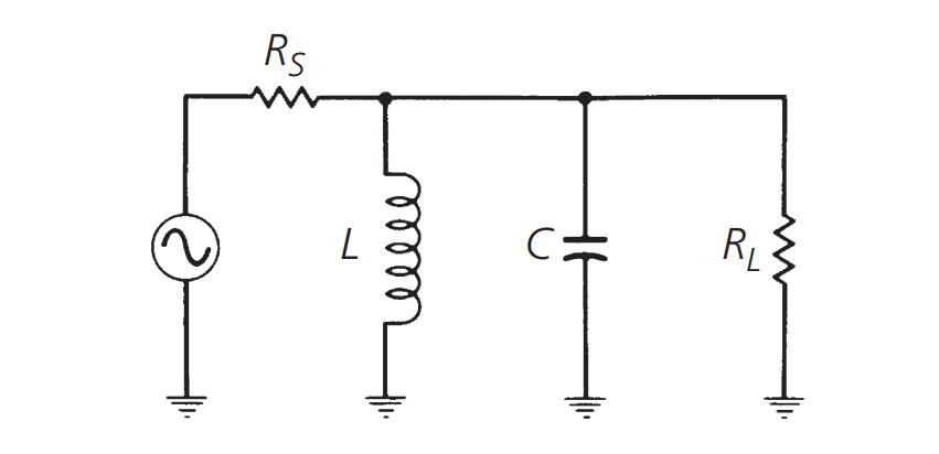
It can be equivalent to:
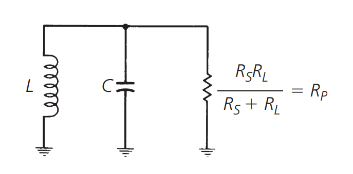
In this case, the load Q can be expressed as:
where \(R_p\) is the equivalent total parallel resistance and \(X_p\) represents reactance/impedance (they are equal at resonance).
e.g. If we want to design a resonant circuit to operate under the conditions of a 150Ω source impedance and a 1000Ω load impedance. At a resonant frequency of 50 MHz, the load Q must be equal to 20. Assuming lossless components and no impedance matching. Then we can obtain \(R_p=130Ω\), according to the formula mentioned above, \(X_p=\frac{R_p}{Q}=\frac{130}{20} =6.5Ω\), and since \(X_p=\omega L=\frac{1}{\omega C}\), we can choose an inductor of 20.7nH and a capacitor of 489.7pF.
It can be seen that reducing \(R_p\) will decrease the Q value of the resonant circuit, and if \(R_p\) remains unchanged, changing \(X_p\) can achieve the same effect. Therefore, for a given source impedance and load impedance, the best Q value of the resonant circuit can be obtained when the inductor is a small value and the capacitor is a large value. In either case, \(X_p\) will decrease. For example:
Therefore, both of these methods can be used to adjust the Q value:
- Select the optimal values for the source impedance and load impedance.
- Select the component values of L and C to optimize Q.
However, in most cases, we can only use the second method because in many cases, the source and load are fixed and cannot be changed. In this case, \(X_p\) is defined by a given Q value, but the calculated value usually does not have a suitable physical value to match it. The solution will be provided in the following text.
Influence of Component Q Values on Load Q
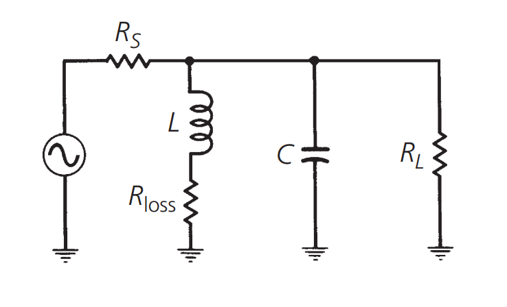
In the previous text, we assumed that the components used in the resonant circuit are lossless, and the Q value of the components does not affect the load Q value. But in non-ideal situations, we must consider the Q value of individual components.
In a lossless resonant circuit, the impedance at the circuit terminals during resonance is infinite. However, in practical circuits, due to component losses, there will be some equivalent parallel resistance:
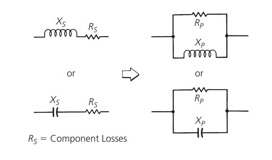
The resistance (Rp) and its related parallel reactance (Xp) can be obtained from
References and Acknowledgements
- "RF-Circuit-Design(second-edition)_Chris-Bowick"
Original: https://wiki-power.com/
This post is protected by CC BY-NC-SA 4.0 agreement, should be reproduced with attribution.This post is translated using ChatGPT, please feedback if any omissions.