Power Solution (Boost) - SX1308
Note: This IC is unstable and not recommended for use.
Project link: https://github.com/linyuxuanlin/Modularity_of_Functional_Circuit/tree/master/Power/SX1308
- Principle: DC/DC (Boost)
- Input Voltage: 2-24 V
- Output Voltage: Up to 28 V
- Output Current: 2 A
- Operating Frequency: 1.2 MHz
- Efficiency: Up to 97%
- Price: ¥0.57
- Features:
- Built-in soft start
- Input undervoltage lockout
- Automatic switch to PFM mode under light load
- Current limiting
- Overheat protection
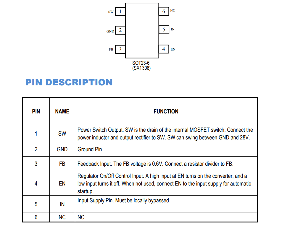
Pin Definitions
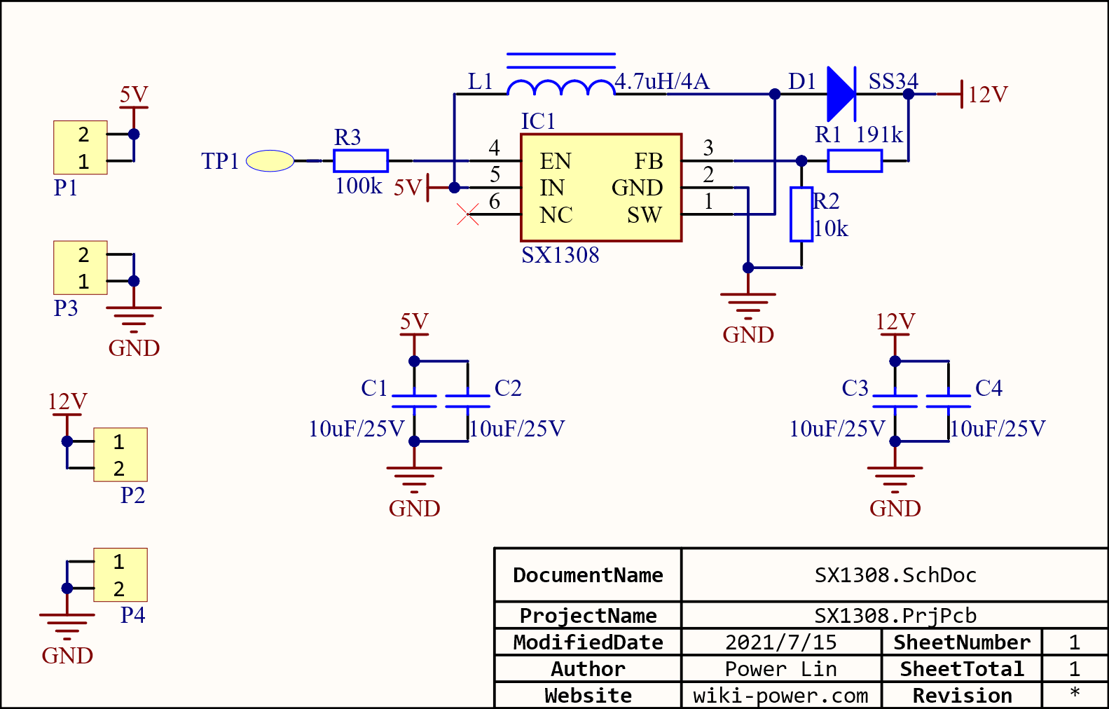
Reference Design
Parameter Adjustment
(For more detailed parameters, please refer to the datasheet)
Output Voltage Adjustment
The output voltage can be set by adjusting the feedback voltage divider resistors \(R_1\) and \(R_2\) (feedback voltage \(V_{REF}=0.6 V\)):
\(V_{OUT}=V_{REF}\times(1+\frac{R_1}{R_2})\)
Generally, when \(R_2\) is selected as 10 kΩ, the relationship between \(V_{OUT}\) and \(R_1\) is as follows:
| \(V_{OUT}\) | \(R_1\) |
|---|---|
| 5 V | 73.2 kΩ |
| 10 V | 158 kΩ |
| 12 V | 191 kΩ |
| 15 V | 240 kΩ |
| 20 V | 324 kΩ |
Enable Pin
EN is the enable pin. It starts when the voltage is above 1.5 V and shuts down when it is below 0.4 V. Do not leave this pin floating.
PCB Layout Reference
- Place the input capacitor close to the IC power pins.
- Place the input and output capacitors close to the IC's GND to minimize the current loop area.
- Widen and shorten the traces for VIN, SW, and VOUT to handle larger AC currents.
- Reduce the copper area around the SW pin of the chip to prevent EMI caused by alternating voltage.
- Shorten the FB trace to prevent noise interference. Place the feedback resistors close to the chip, and the GND of R2 should be placed as close as possible to the GND pin of the IC. The routing from VOUT to R1 should be far away from inductors and switch nodes.
Pitfall Summary
- The reference schematic in the Chinese datasheet may have a mistake with the 15 pF NP0 capacitor, which should be a grounded filtering capacitor (it can also be omitted). If not removed, it cannot handle heavy loads.
- Refer to the technical post http://www.crystalradio.cn/thread-1497661-1-1.html.
- This circuit is greatly affected by PCB layout. There should not be excessive copper area around the SW pin to avoid parasitic capacitance. Other layout considerations should strictly follow the above recommendations.
- The measured maximum output current under load is around 800 mA, which can maintain a stable output voltage (11.6 V).
- The EN pin must not be left floating. It must be pulled up (to enable Boost) or pulled down (to disable it), otherwise it will output at the original voltage.
Original: https://wiki-power.com/
This post is protected by CC BY-NC-SA 4.0 agreement, should be reproduced with attribution.This post is translated using ChatGPT, please feedback if any omissions.