Communication Protocols - Digital Logic Levels
TTL Logic Levels

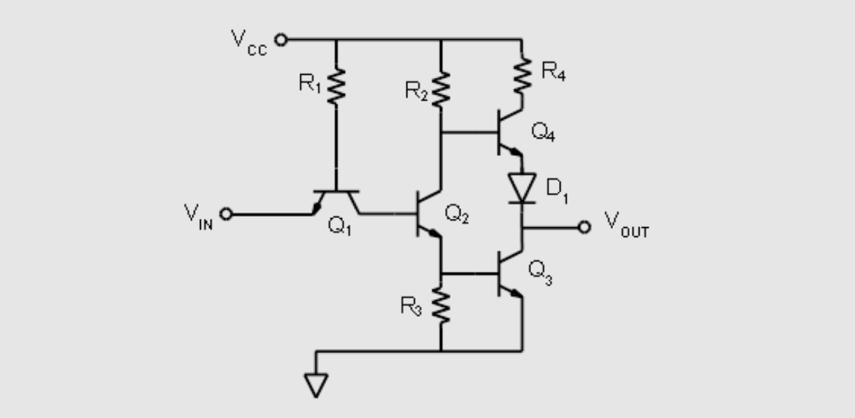
TTL (Transistor-Transistor Logic) is based on a transistor structure, with a standard power supply of 5V. Due to the large gap between 2.4V and 5V, voltage fluctuations can increase system power consumption. To address this, LVTTL (Low Voltage Transistor-Transistor Logic) levels were developed, including 3.3V and 2.5V LVTTL.
Characteristics of (LV)TTL levels:
- TTL circuits use current-controlled devices, resulting in fast circuit speed and short transmission delay (5-10ns), but high power consumption.
- TTL levels generally have significant overshoot, which can be mitigated by adding a 22Ω/33Ω resistor at the starting end.
- When a TTL input pin is left floating, it is internally considered as a high level. To pull it down, a resistor below 1k should be connected.
- The speed of TTL level interfaces is generally limited to within 30MHz. This is because the input end of the BJT has a relatively large input capacitance of a few pF (forming a LPF). If the input signal exceeds a certain frequency, the signal will be lost.
- The driving capability of TTL levels is generally up to several tens of milliamperes. The normal operating voltage of the signal is generally high. If it is close to an ECL circuit with a lower signal voltage, significant crosstalk issues may arise.
CMOS Logic Levels

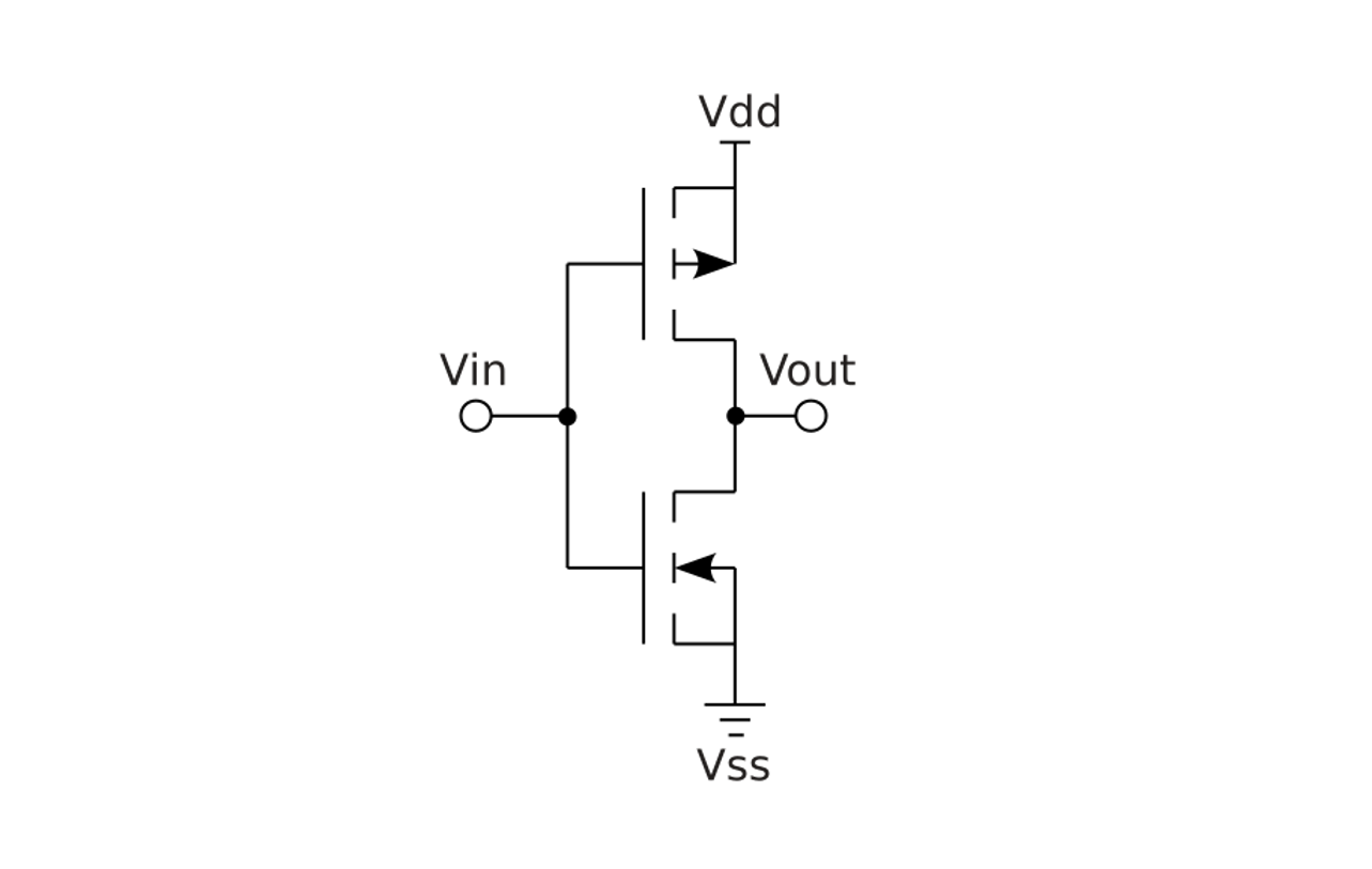
CMOS (Complementary Metal Oxide Semiconductor) is based on the structure composed of NMOS and PMOS, with a standard power supply of 5V. Similar to TTL, CMOS also has LVCMOS level standards. However, due to the lower threshold voltage of MOS transistors compared to BJTs, LVCMOS can use lower voltage for communication. LVCMOS has standards of 3.3V, 2.5V, 1.8V, 1.5V, and 1.2V.
Characteristics of (LV)CMOS levels:
- CMOS circuits use voltage-controlled devices, resulting in slower circuit speed and longer transmission delay (25-50ns), but lower power consumption. However, at high switching frequencies, CMOS series actually consume more power than TTL.
- CMOS interfaces have larger noise margins and higher input impedance compared to TTL interfaces. Under normal circumstances, CMOS has better power consumption and anti-interference capabilities than TTL.
- CMOS structures have parasitic thyristor structures internally. When the input or input pin exceeds a certain value above VCC (e.g., 0.7V for some chips), if the current is large enough, it may cause latch-up and burn out the chip.
- CMOS circuits have high input impedance, so the capacitive load can be small and does not require large electrolytic capacitors. Since CMOS circuits usually have weak driving capability, they must be converted to TTL before driving ECL circuits. In addition, when designing CMOS interface circuits, it is important to avoid excessive capacitive loads, as this will slow down the rise time and increase the power consumption of the driving device (because capacitive loads do not consume power).
Comparison of Different Level Standards
Digital circuits have a dual threshold standard. Although only two states, 0 and 1, are ultimately represented, the voltage at which 0 is considered and the voltage at which 1 is considered are agreed upon through the dual threshold standard.
| \(VCC\) | \(V_{OH}\) | \(V_{IH}\) | \(V_{IL}\) | \(V_{OL}\) | \(GND\) | |
|---|---|---|---|---|---|---|
| 5V TTL | 5.0 | 2.4 | 2.0 | 0.8 | 0.4 | 0.0 |
| 3.3V LVTTL | 3.3 | 2.4 | 1.5 | 0.8 | 0.4 | 0.0 |
| 5V CMOS | 5.0 | 4.5 (0.9*VCC) | 3.5 (0.7*VCC) | 1.5 (0.3*VCC) | 0.5 (0.1*VCC) | 0.0 |
| 3.3V CMOS | 3.3 | 2.97 (0.9*VCC) | 2.31 (0.7*VCC) | 0.99 (0.3*VCC) | 0.33 (0.1*VCC) | 0.0 |
| 2.5V CMOS | 2.5 | 2.0 | 1.7 | 0.7 | 0.4 | 0.0 |
| 1.8V CMOS | 1.8 | 1.35 | 1.17 | 0.63 | 0.45 | 0.0 |
Serial and Parallel Communication
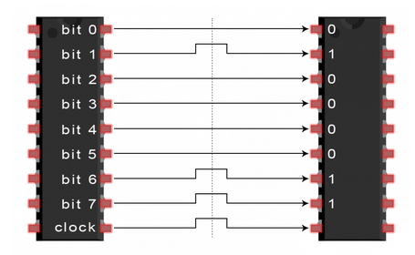
Data can be transmitted in parallel or serial form. In parallel communication, the data bits are sent simultaneously, each through a separate line. The following diagram shows the parallel transmission of the letter 'C' in binary (01000011):

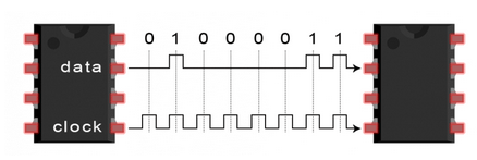
In serial communication, the bits are sent one by one through a single line. The following diagram shows the serial transmission of the letter 'C':

References and Acknowledgements
- "Analog Engineer’s Pocket Reference"
- Understanding the Working Principle, Advantages, Disadvantages, and Application Cases of SPI Bus
- [FPGA13][Circuit] Interface Voltage Standards
Original: https://wiki-power.com/
This post is protected by CC BY-NC-SA 4.0 agreement, should be reproduced with attribution.This post is translated using ChatGPT, please feedback if any omissions.