Common Tips for AD
- Organized and compiled some practical tips.
Schematic Library Section
Underlining Pin Names (Active Low)
Method: Add a backslash "\" after each letter that needs underlining.
Example: RESET with underlines - R\E\S\E\T
PCB Footprint Library Section
(To be updated)
Schematic Section
Disabling "Add Room" Operation
Reason: The Room operation is useful for multi-channel routing, allowing you to apply wiring within one channel directly to other channels. For single-channel designs, Room is not necessary.
Method:
- Menu Bar - Project - Project Options - Class Generation tab.
- Uncheck "Generate Room."
PCB Section
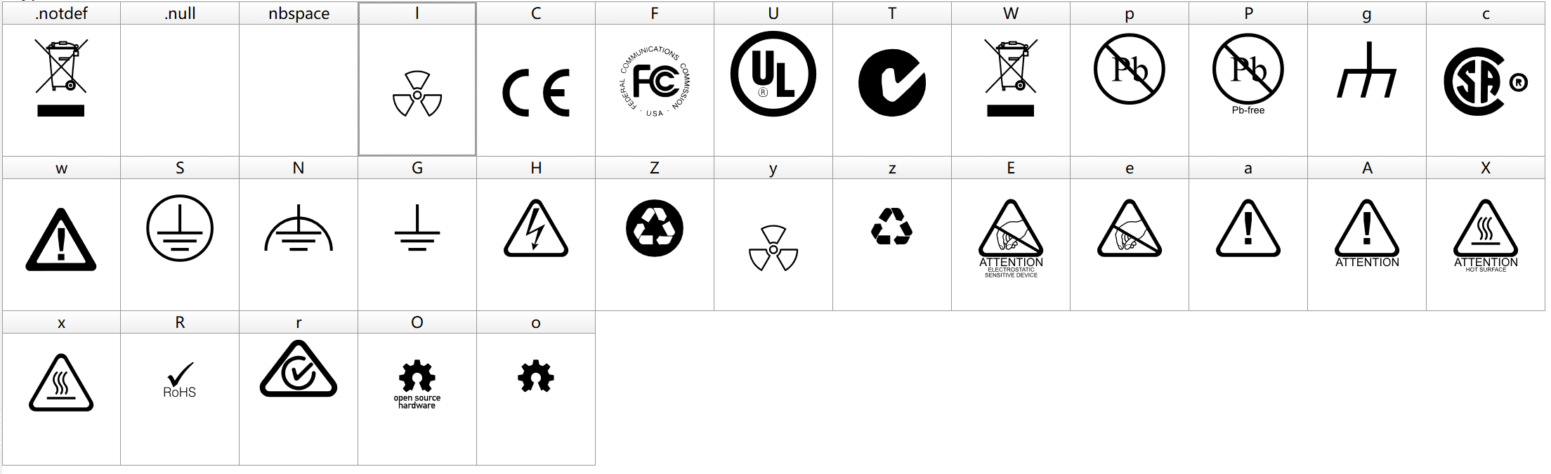
Adding Logo and Labels
Reason: If you import images directly, the created logo cannot be freely resized.
Method: Use the Font Creator software, download my font library as a template from GitHub, and create your custom font library. After making the font library, install the .ttf file, and you can use the corresponding characters to insert the logo in Altium.
Characters corresponding to the logo are as follows:
Auto-arranging Components within a Defined Area
Reason: When transferring the schematic to the PCB, some components may move far from their intended positions.
Method: Select All - TOL - Draw a box.
Circular Array Layout
Method:
- Select objects - Copy.
- EA - Check "Paste to Current Layer."
- Click "Paste Array" - Set the number of objects and spacing.
Quick Via Change and Layer Switch
Method: Use the numeric keypad + / - to toggle vias during routing.
Uniformly Set Via Net Properties
Method:
- Right-click any via without properties - Find Similar Objects - Set Net to "Same."
- In the Properties panel, uniformly add via net properties.
Adding Teardrops
Reason: Teardrops enhance signal integrity, reduce signal loss and reflections, and reduce the risk of wire-to-via contact breakage during external force impacts.
Method: Use the shortcut key TE.
Solder Mask Window
Reason: Solder mask windows can enhance current carrying capacity.
Method: Copy the desired trace, and paste it into the respective Top/Bottom Solder layer.
Operations in 3D Preview
Method:
- Press the number key "3" to enter 3D preview mode.
- Press the number key "2" to return to PCB editing.
- Press the number key "0" to restore the default view.
- Ctrl + F to flip.
- Ctrl + scroll wheel to zoom.
- Shift + right-click to change the view.
Preserving Net Properties During Copy-Paste
Reason: When copying and pasting objects with electrical properties, net properties are lost.
Method: Copy the object - EA - Check "Keep Net Names" - Paste.
Outputting Solder Pad Numbers
(To be updated)
How to Create Slots on the PCB
On the Mechanical 1 Layer of the PCB, draw a closed shape for the slot, select it, and use the shortcut keys T - V - B to generate the slot (it's best to switch to 3D view for confirmation).
References and Acknowledgments
Original: https://wiki-power.com/ This post is protected by CC BY-NC-SA 4.0 agreement, should be reproduced with attribution.
This post is translated using ChatGPT, please feedback if any omissions.