Semiconductor Testing Fundamentals - DC Parameter Testing
DC parameter testing primarily focuses on the characteristics of individual pins on a semiconductor device. For most DC parameters, the essence lies in measuring the resistivity of the semiconductor, which is explained using Ohm's Law. To validate the feasibility of the DC testing process, one can use a resistor to equivalently replace the Device Under Test (DUT) to eliminate issues external to the DUT. For instance, consider a parameter like VOL that appears in the chip's specification:
| Parameter | Description | Test Conditions | Min | Max | Units |
|---|---|---|---|---|---|
| VOL | Output LOW Voltage | VDD = Min, IOL = 8.0mA | 0.4 | V |
We can observe that the maximum VOL is 0.4V, and IOL is 8mA. This means that when producing an output logic low level, it must generate an 8mA current at a voltage not exceeding 0.4V. Consequently, we can deduce that the maximum resistance of this device does not exceed 50Ω. Therefore, we can use a resistor not exceeding 50Ω to substitute for the DUT to verify the testing process. Our goal is to focus on issues related to the DUT rather than those outside of it.
IDD & Gross IDD
IDD represents the current from the drain (D) to the drain (D) in CMOS circuits, or it is referred to as ICC in TTL circuits (current from collector to collector). Gross IDD refers to the total current flowing into the VDD pin (testable in the Wafer Probe or final product stages). IDD checks if the chip's total current exceeds the specified limits, typically considering current at the lowest power consumption and the maximum operating frequency.
Testing Gross IDD is crucial to determine whether DUT testing can proceed. This test usually follows the OS (Operating System) test and is the first test performed after powering the DUT. If Gross IDD testing fails (e.g., due to excessive current), further testing cannot continue.
During the Gross IDD testing stage, it is not known if pre-processing can proceed normally, so IDD specifications need to be relaxed. Once Gross IDD testing passes, pre-processing can be carried out to precisely define IDD specification current.
Gross IDD testing begins with a reset to set all input pins to low or high levels. Typically, VIL is set to 0V, VIH is set to VDD, and all output pins are left open (to prevent floating and leakage current, which could increase IDD). The schematic for the test is as follows:
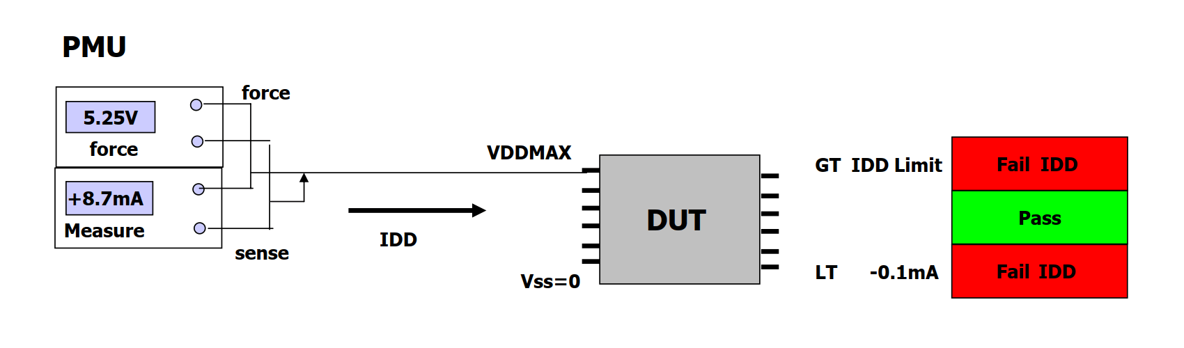
Important considerations include:
- The current clamp must be set to prevent damage to the testing equipment due to excessive current.
- If negative current occurs, it also indicates a test failure.
- If a test error occurs, you can first rule out problems with the testing equipment by running the test without the chip in the socket; the current should be 0. If not, it means that devices outside the DUT are also consuming current.
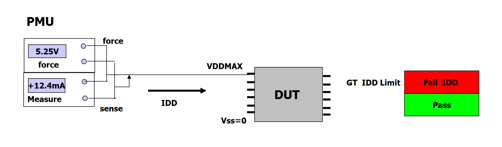
IDD Testing - Static Method
Static IDD testing measures the total current flowing into the VDD pin when the DUT is operating in its lowest power consumption mode. The difference between static IDD and Gross IDD testing is that Gross IDD does not involve pre-processing; it is a rough test. In contrast, static IDD testing involves a pre-processing mode before conducting the test.
For example, consider the following IDD parameter sample:
| Parameter | Description | Test Conditions | Min | Max | Units |
|---|---|---|---|---|---|
| IDD Static | Power Supply Current | VDD = 5.25V, inputs = VDD, Iout=0 | +22 | µA |
The schematic for static IDD testing is as follows:

The testing process is as follows:
- Set the DUT to consume the least current and remain in a static state using test vectors.
- Measure the pin current values:
- Above IDD Spec: Fail
- In any other range: Pass
During testing, it's typically necessary to introduce a delay between powering up and sampling to allow parasitic capacitance to charge fully and prevent interference.
If you need to test static current under different logic conditions, you can measure the IDDQ parameter, increasing the test coverage (IDDQ measures current under a specific static logic state, for example, testing a subset of MOS transistors in a particular state).
IDD Testing - Dynamic Method
The purpose of IDD dynamic testing is to measure the current consumed by the DUT when it's executing functions dynamically (usually at the DUT's maximum operating frequency) to ensure it doesn't exceed the nominal value.
For example, the table below provides a sample of dynamic IDD parameters:
| Parameter | Description | Test Conditions | Min | Max | Units |
|---|---|---|---|---|---|
| IDD Dynamic | Power Supply Current | VDD = 5.25V (commercial), f = f_max (66MHz) | +18 | mA |
Illustration of the testing process:
The testing process is similar to the static method.
VOL/IOL & VOH/IOH
VOL represents the highest voltage (V) limit when outputting a low level (L) (not recognized as logic 1). IOL represents the drive capability of the pin's output current (I, sink) when outputting a low level (L). Together, they measure the impedance of the pin buffer when outputting a low level, ensuring it can sink a constant current at the appropriate output voltage.
VOH represents the lowest voltage (V) limit when outputting a high level (H) (not recognized as logic 0). IOH represents the drive capability of the pin's source current (I) when outputting a high level (H). Together, they measure the impedance of the buffer when outputting a high level, ensuring it can source a constant current at the appropriate output voltage.
For example, the table below provides VOL/IOL & VOH/IOH parameters for a 256 x 4 Static RAM:
| Parameter | Description | Test Conditions | Min | Max | Units |
|---|---|---|---|---|---|
| VOL | Output LOW Voltage | VDD = 4.75V, IOL = 8.0mA | 0.4 | V | |
| VOH | Output HIGH Voltage | VDD = 4.75V, IOH = -5.2mA | 2.4 | V |
Testing VOL/IOL & VOH/IOH mainly aims to verify whether VOL/VOH reaches the correct voltage levels when applying sourcing or sinking current (whether they can meet the voltage threshold under a specific current output). There are static and dynamic testing methods. The static method involves applying current to the pins and then measuring the voltage one by one, while the dynamic method introduces VREF during functional testing to create a dynamic load current before measuring the voltage.
VOL/IOL Testing - Serial Static Method
The testing schematic for measuring VOL/IOL using the serial static method is as follows:
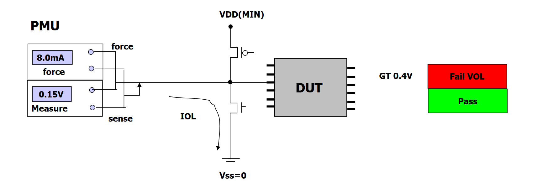
The testing process is as follows:
- Initially, the pins to be tested need to be set to a low-level output through pre-processing.
- Apply a constant IOH to the pins, and wait for 1-5 milliseconds before measurement (adjust the delay in the PMU).
- Measure the pin voltage:
- Above VOL (+0.4V): Fail
- In any other range: Pass
Important considerations:
- IOL is a positive current value because it flows from the PMU to the DUT.
- Since a constant current is applied, a voltage clamp needs to be set. If the measured voltage is lower than the clamped voltage, it may be due to the logic being set to a high level, triggering forward biasing of the power protection diode.
- The parameter VDDmin represents the minimum supply voltage that allows the DUT to function properly during testing. If it goes below this threshold, accurate test results cannot be obtained.
VOH/IOH Test - Serial Static Method
The schematic diagram for measuring VOH/IOH using the serial static method is shown below:
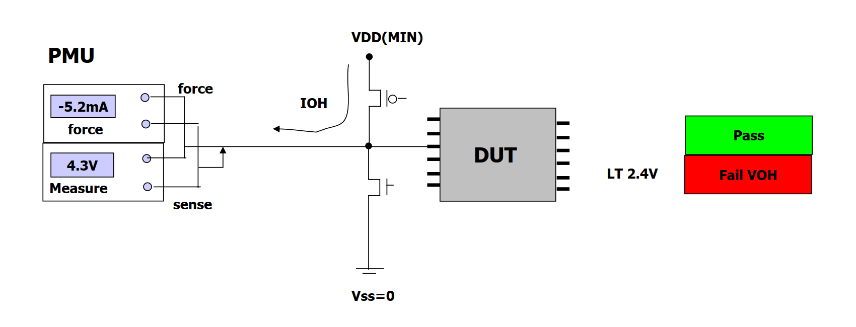
The testing process is as follows:
- Begin by pre-processing to set the pin to be tested as a high-level output.
- Apply a constant IOH to the pin, and wait for 1-5 milliseconds before measuring (adjust delay in the PMU).
- Check the pin voltage:
- Below VOH (+2.4V): Fail
- In other ranges: Pass
Important notes:
- IOL is negative because it flows from PMU to DUT.
- Since a constant current is applied, a voltage clamp needs to be set. If the measured voltage is higher than the clamped voltage, it may be due to the pin logic being set to a low level, triggering forward biasing of the protection diode.
- VDDmin represents the minimum supply voltage required for proper testing of the DUT. Going below this threshold will result in inaccurate test results.
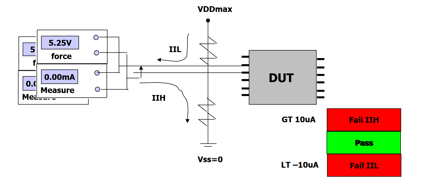
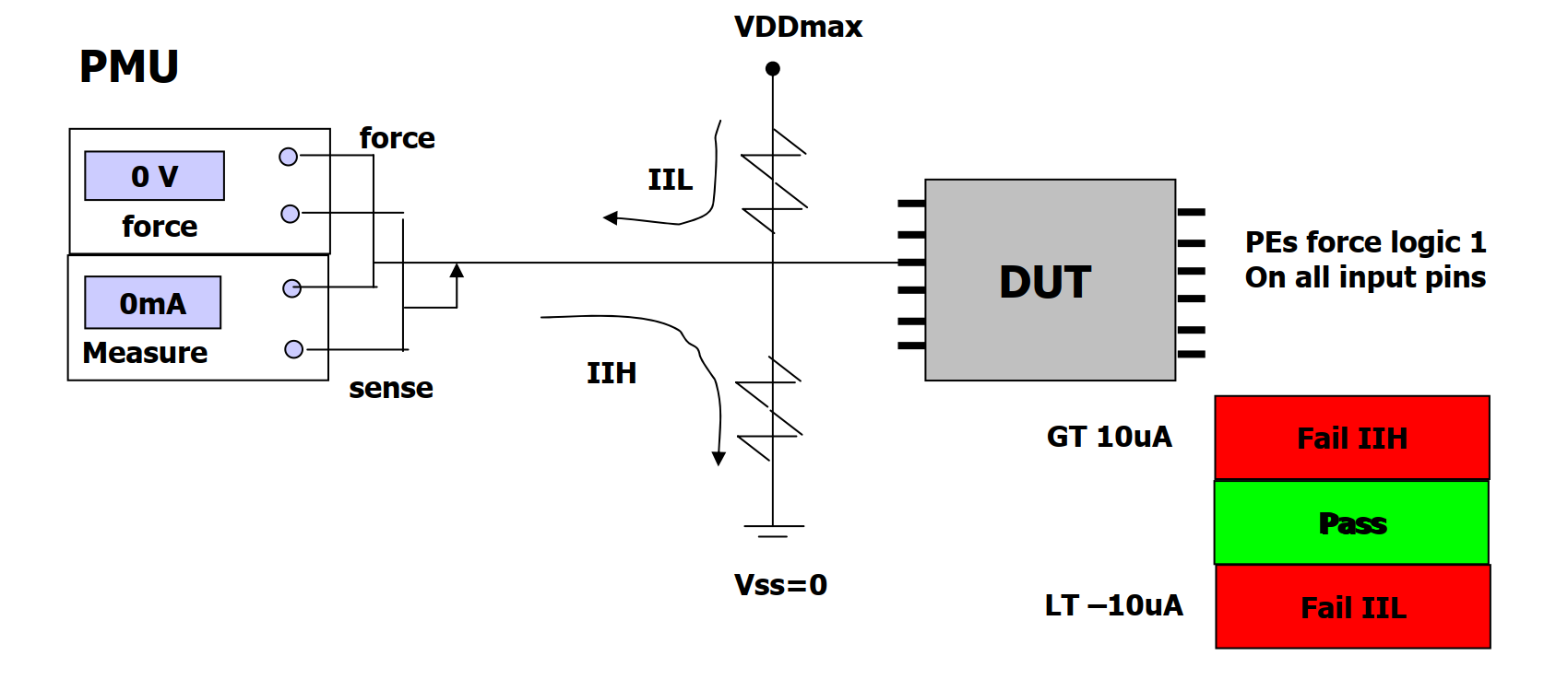
IIL/IIH
IIL refers to the maximum input leakage current (I, source, from external to DUT's VSS) allowed when the input pin (I) is at a low logic level (L). It is used to check if the pin's leakage current to the power source exceeds the specified limit and assess the isolation level. IIH refers to the maximum input sinking current (I, sink, from DUT's VDD to the external pin) allowed when the input pin (I) is at a high logic level (H). For example, the table below shows the IIL and IIH parameters for a 256 x 4 Static RAM:
| Parameter | Description | Test Conditions | Min | Max | Units |
|---|---|---|---|---|---|
| IIL, IIH | Input Load Current | VSS ≤ Vin ≤ VDD(5.25V) | -10 | +10 | µA |
IIL measures the resistance from input pins to VDD, while IIH measures the resistance from input pins to VSS. This test ensures that input impedance meets design requirements and that input current stays within limits. IIL/IIH can be tested using serial, parallel, or merged methods or through functional testing. Serial testing examines pins one by one, which is accurate but relatively time-consuming.
Additionally, IIL/IIH tests are typically performed only on pure input pins. If bidirectional pins are encountered, an output load should be added to stabilize the voltage level, preventing current from flowing into protection devices and affecting test results.
IIL/IIH Test - Serial Static Method
The schematic diagram for testing input pin IIL using the serial method is shown below:
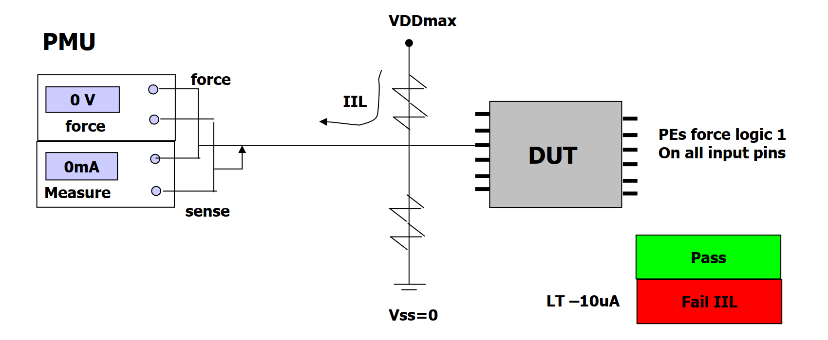
The testing process is as follows:
- Begin by supplying the DUT with a VDDmax (worst-case scenario) power source.
- Set all input pins of the DUT to a high logic level (VIH).
- Use the PMU to pull a single input pin down to VSS.
- Wait for 1-5 microseconds and measure the current:
- Below IIL (-10µA): Fail (current into the DUT exceeds the limit)
- In other ranges: Pass
The schematic diagram for testing input pin IIH using the serial method is shown below:
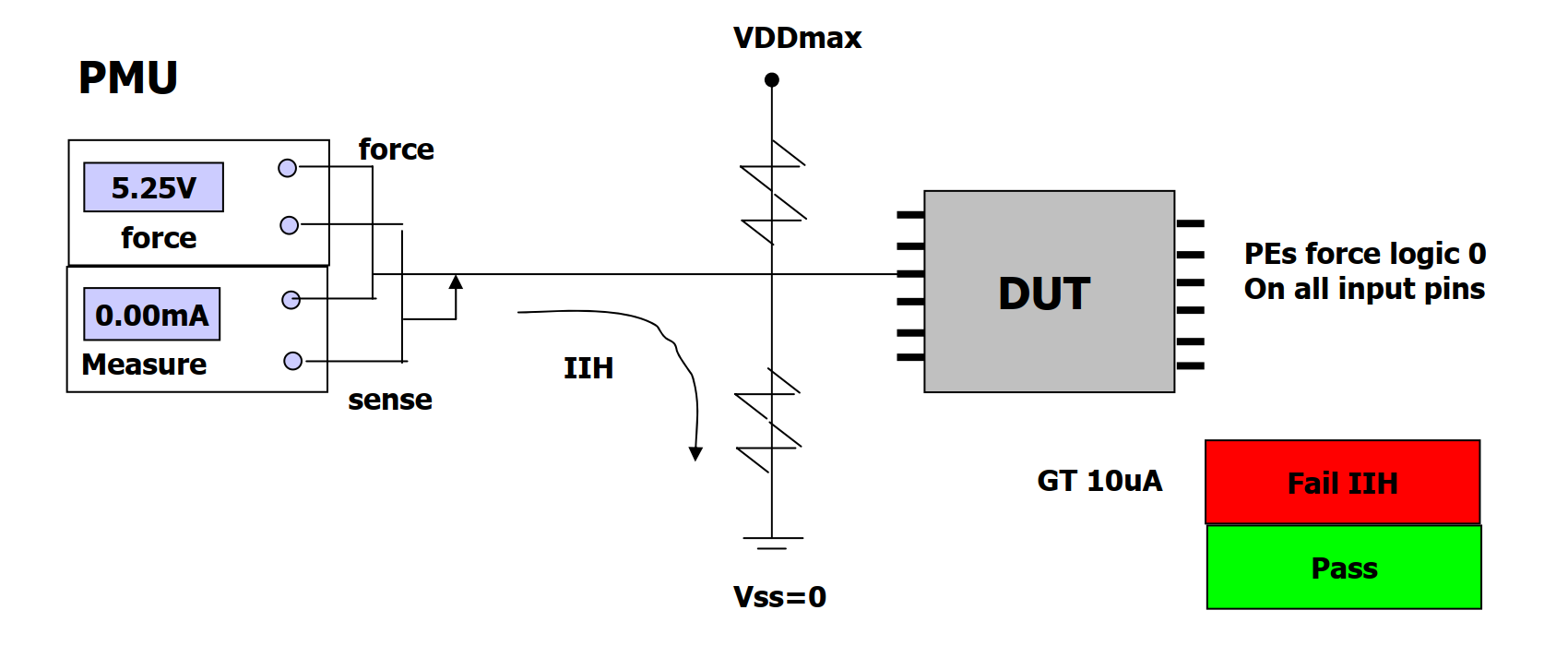
The testing process is as follows:
- Begin by supplying the DUT with a VDDmax power source.
- Set all input pins of the DUT to a low logic level (VIL).
- Use the PMU to pull a single input pin up to VDDmax.
- Wait for 1-5 microseconds and measure the current:
- Above IIH (+10µA): Fail (current out of the DUT exceeds the limit)
- In other ranges: Pass
IIL/IIH Test - Parallel Static Method
In certain testing systems, it is possible to perform parallel leakage current measurements, a method known as the "Parallel Test Method." Parallel leakage current measurement involves utilizing multiple PMUs to measure the current on multiple pins simultaneously. All input pins are forced to a high state, and the current on each pin is measured in parallel. Subsequently, the test results are compared to the nominal values to draw conclusions.
- Firstly, supply the DUT with a power source of VDDmax.
- Use multiple PMUs to force each input pin to a high state at VDDmax (for IIH measurement).
- Wait for 1 to 5 microseconds, detect the current, and draw conclusions based on the comparison.
- Then, pull the pins down to VSS and repeat the above steps for IIL measurement.
The key feature of the parallel method is the ability to measure the current of each pin individually simultaneously, enabling rapid completion of IIL/IIH testing. However, a drawback is that it's more challenging to detect leakage between input pins since all inputs are held at the same level.
IIL/IIH Testing - Combined Static Method
The combined test method, also known as the "Ganged Method," involves combining all input pins into one pin and measuring the total leakage current with a single PMU. The testing concept is illustrated below:
The combined testing method is similar to the previous one. The total current limit is the nominal value of a single pin. If the test result exceeds this limit, it requires a switch back to serial testing. This testing method is particularly effective for CMOS devices (high-impedance inputs).
IOZL/IOZH
High-impedance current, IOZ, refers to the leakage current when the output pin (O) is in the high-impedance state (Z). Specifically, IOZL is the leakage current when the pin is at a low level (L), while IOZH is the leakage current when it's at a high level (H). This parameter is used to assess whether there is excessive leakage current when the pin is in the off state.
This parameter ensures that bidirectional or high-impedance output pins can be properly turned off (set to high-impedance state). IOZL measures the pin's resistance to VDD when it's in the high-impedance state, while IOZH measures the resistance to VSS. Typically, it is represented as follows in the datasheet:
| Parameter | Description | Test Conditions | Min | Max | Units |
|---|---|---|---|---|---|
| IOZ | Output Current High-Z | VSS ≤ Vout ≤VDD(5.25V), Output Disabled | -2.0 | +2.0 | µA |
IOZL/IOZH Testing - Serial Static Method
The serial static testing of IOZL/IOZH is illustrated as follows:
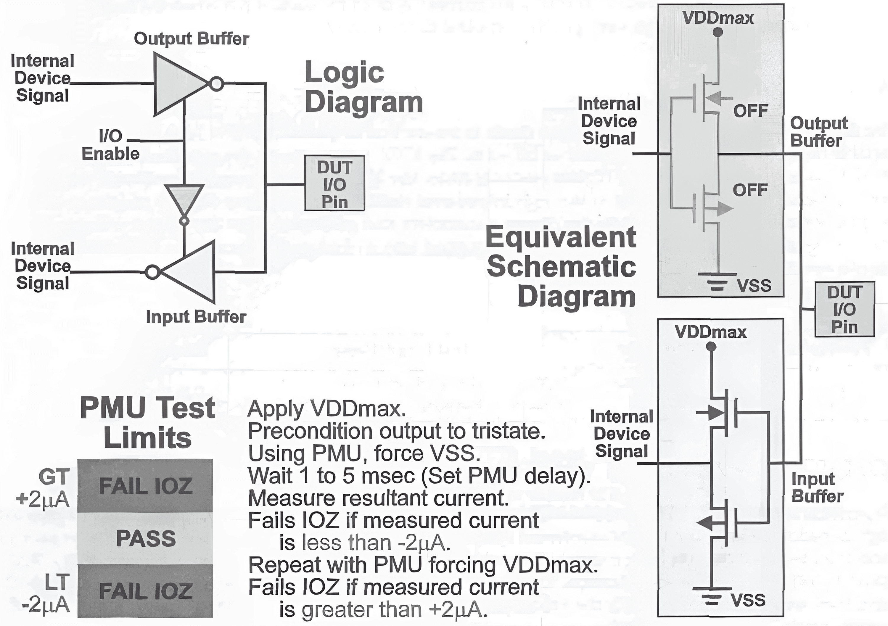
The testing process is as follows:
- First, provide the device with a power source of VDD.
- Set the device's pins to a high-impedance state and use a PMU to forcibly pull the pins high/low.
- Measure the current on the pins.
- Below -IOZ (-2µA): Fail
- Above +IOZ (+2µA): Fail
- In other ranges: Pass
The advantage of serial testing is the ability to accurately measure the current of individual pins, but it is slower. Additionally, this testing requires setting clamp currents.
IOZL/IOZH Testing - Parallel Static Method
The parallel static method involves using multiple PMUs simultaneously on multiple pins. Further details on this method are not discussed here, but its advantage is speed.
VI (Input Clamp)
The input clamp VI refers to the voltage measured on the input pin (I) of TTL devices (non-CMOS) when a negative current (current extraction) is applied. This test serves to verify the integrity of the transistor's emitter and the diode clamped between it and ground. It is represented in the datasheet as follows:
| Parameter | Description | Test Conditions | Min | Max | Units |
|---|---|---|---|---|---|
| VI | Input Clamp Voltage | VCC = Minimum, Iin = -18mA | +1.5 | V |
VI Test - Serial Static Method
VI is measured using the serial static method, and the test schematic is as follows:
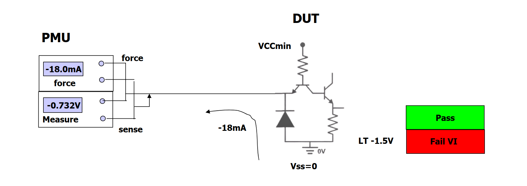
The test procedure is as follows:
- First, ensure that this is an input pin of a TTL device, and apply VCCmin power to it.
- After setting the voltage clamp, use the PMU to extract a current of -15mA to -20mA.
- Measure the voltage on the pin.
- Below VI (-1.5V): Fail
- In other ranges: Pass
IOS (Short-Circuit Output Current)
The short-circuit output current represents the current (I) generated when the output pin (O) is short-circuited (S) under specific conditions. The purpose is to measure the output impedance when the pin outputs a high level but is shorted to zero voltage, ensuring that the output current is not too high under the worst load conditions. It also indicates the maximum instantaneous current that the DUT pin can provide for charging capacitive loads, which can be used to calculate the rise time. IOS is specified as follows:
| Parameter | Description | Test Conditions | Min | Max | Units |
|---|---|---|---|---|---|
| IOS | Output Short Circuit Current | Vout = 0V, VDD = 5.25V, *Short only 1 output at a time for no longer than 1 sec | -85 | -30 | mA |
IOS Test - Serial Static Method
The test schematic is as follows:
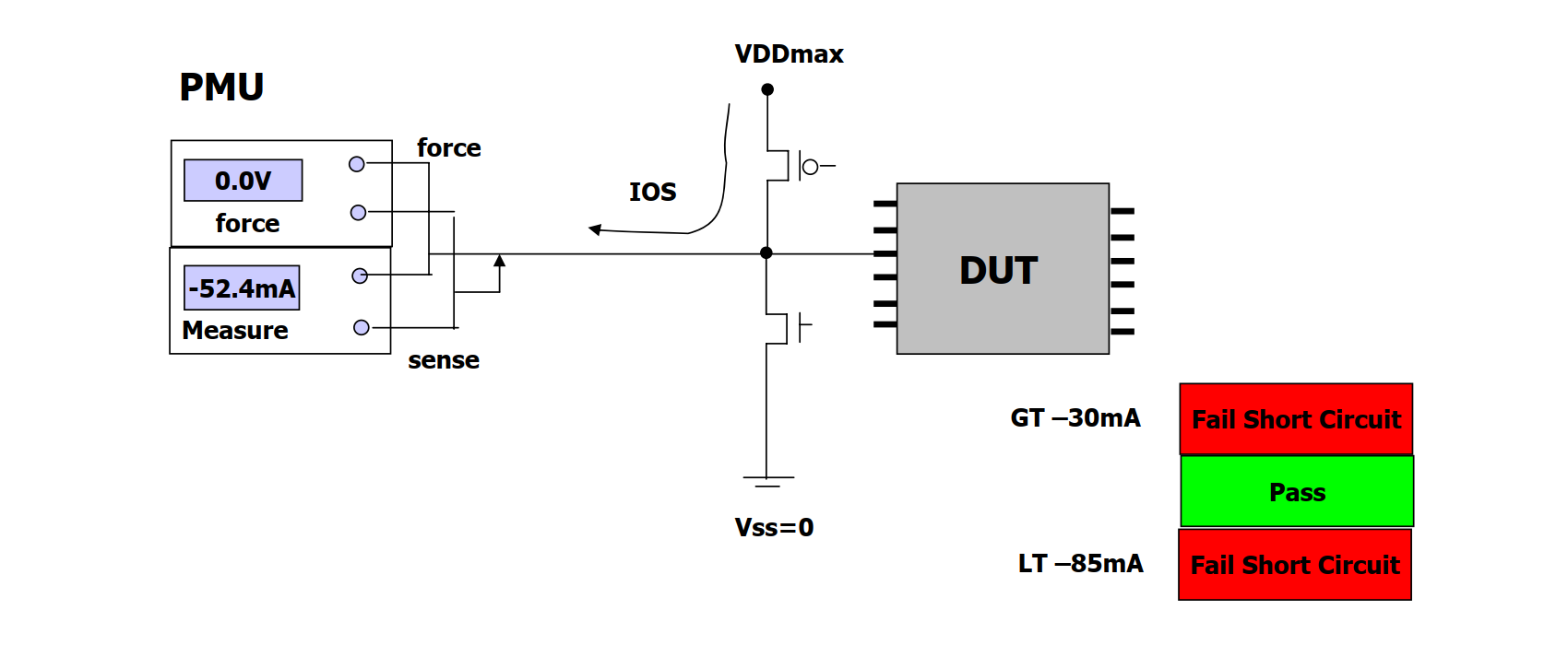
The test procedure is as follows:
- Apply power to VDDmax, precondition the device to make the pin output a high level.
- Use the PMU to pull the pin down to 0V, measure the output current, and compare it with the nominal value to draw a conclusion.
In the testing of IOS, a reasonable logic is needed to avoid hot switching. First, set the PMU to voltage measurement mode with a forced zero current, connect it to the DUT output, measure and save the DUT's VOH voltage. Then, disconnect and set the PMU to pull up to the VOH voltage just measured, then reconnect to the DUT (at this point, both ends have VOH voltage), and then lower the PMU to 0V to measure the current value. After the measurement is complete, the PMU must be raised back to VOH before disconnecting. This ensures that the voltages at both ends are consistent during relay switching.
Factors that may cause the test to fail:
- Exceeding the upper limit
- High output impedance, resulting in an insufficient absolute current.
- The fixture itself has resistance.
- No proper preconditioning.
- Below the lower limit
- Low output impedance, resulting in an excessively high absolute current.
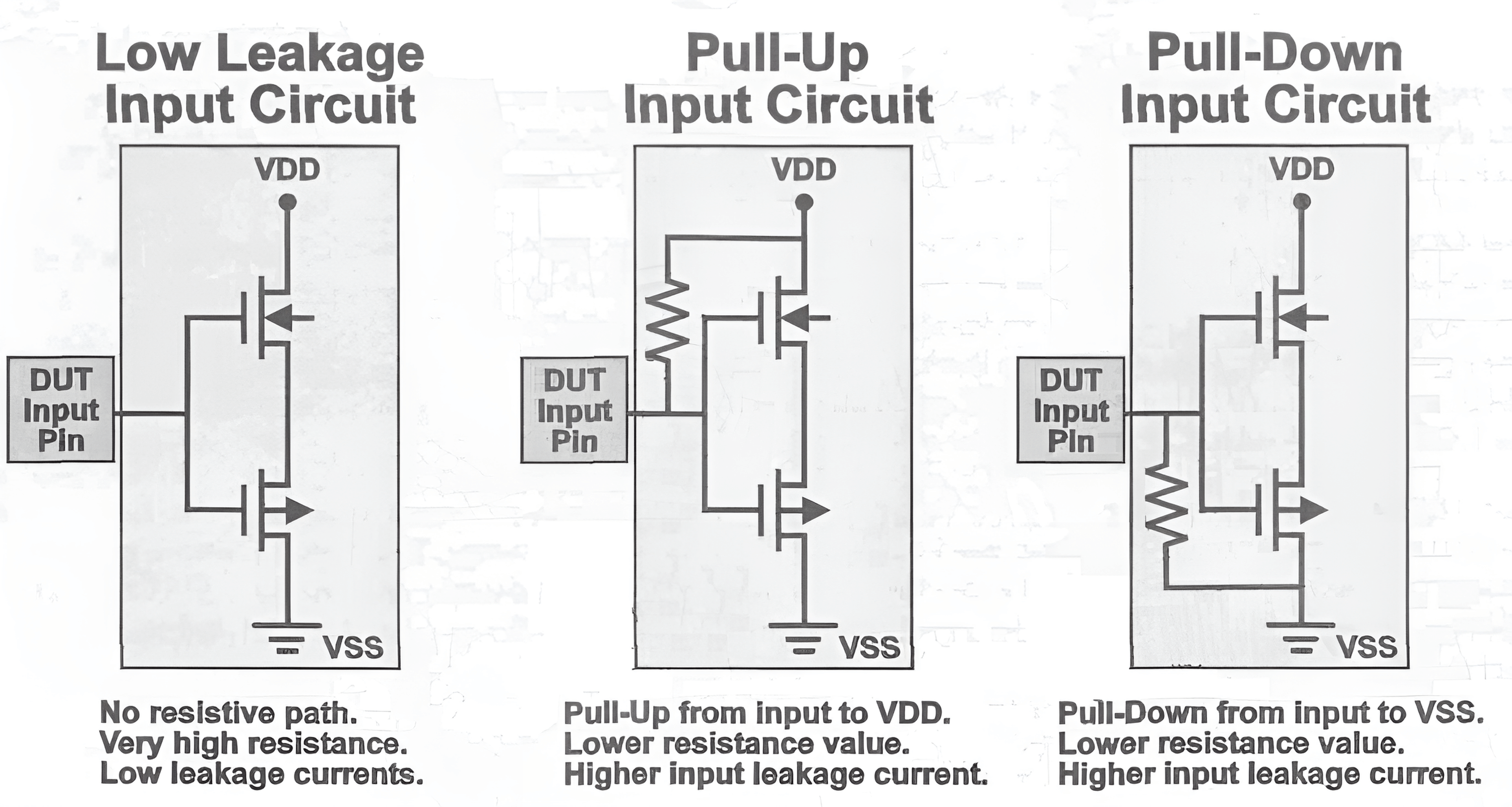
Resistive Inputs (Pull-Up/Pull-Down Resistor Inputs)
Some input pins may have active pull-up and pull-down structures, and it is essential to ensure that the input buffer's pull-up and pull-down resistor paths are functioning correctly. Testing must be performed serially, as the internal pull-up/pull-down structures may vary between different pins. An illustrative diagram of pin structures is provided below:
Output Fanout Capability
The fanout capability refers to the ability of an output pin to drive multiple input pins based on its voltage and current parameters. In other words, it measures the ability of an output pin to handle multiple input pins, also known as the pin's driving capacity.
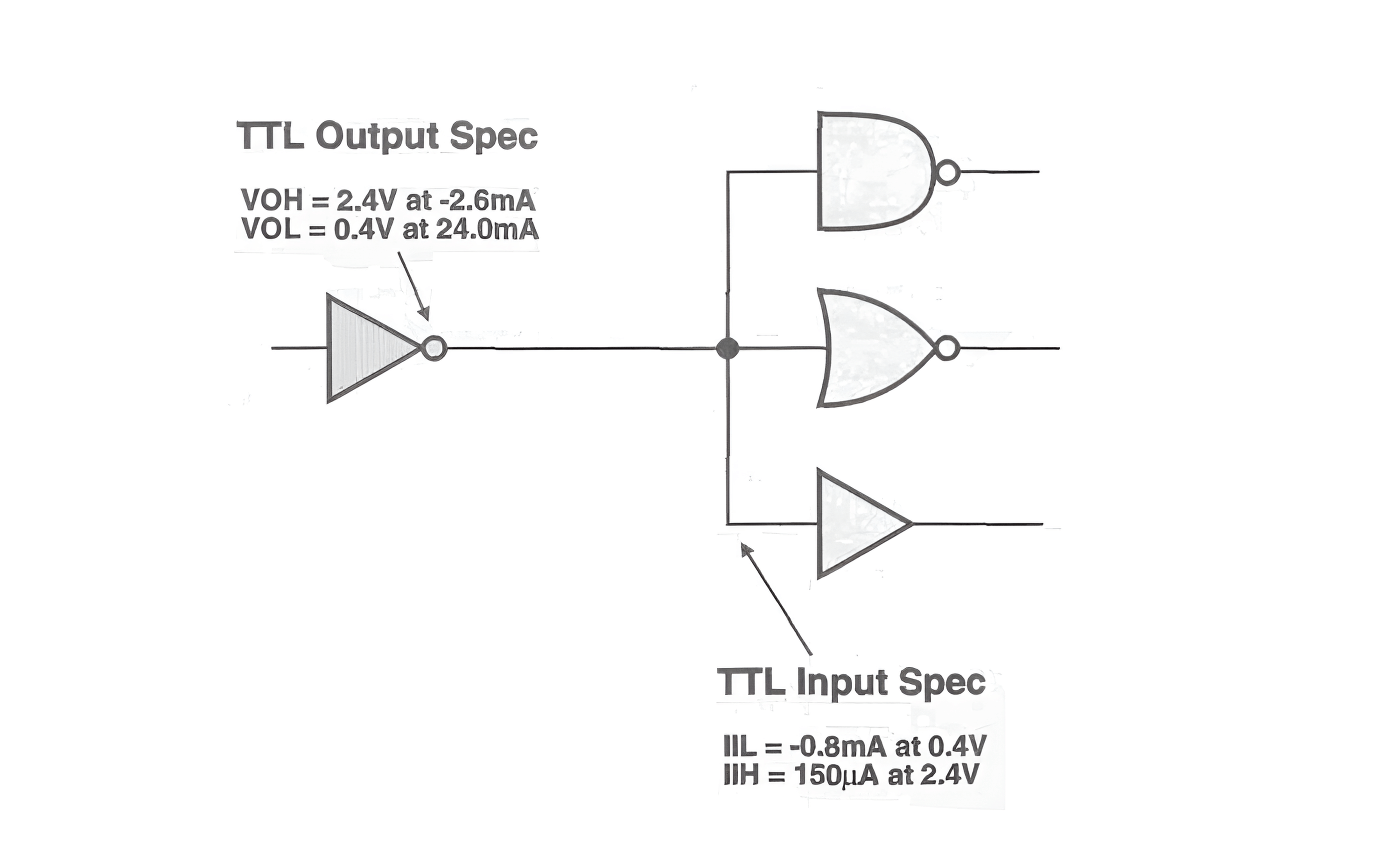
As shown in the above figure, this TTL output can drive approximately 17 input pins to a high state or 30 input pins to a low state. In the datasheet, the pin parameters are typically represented as follows:
| Parameter | Description | Test Conditions | Min | Max | Units |
|---|---|---|---|---|---|
| VOH | Output HIGH Voltage | VCC = 4.75V, IOH = -2.6mA | 2.4 | V | |
| VOL | Output LOW Voltage | VCC = 4.75V, IOH = 24mA | 0.4 | V | |
| IIL | Input LOW Load Current | Vin = 0.4V | -800 | µA | |
| IIH | Input HIGH Load Current | Vin = 2.4V | 150 | µA |
The fanout capability varies significantly between TTL and CMOS devices. This is because CMOS devices have high input impedance, theoretically allowing a CMOS output to drive multiple CMOS inputs. However, CMOS input pins have parasitic capacitance, and the more inputs are connected, the larger the capacitance becomes. This can lead to delay due to capacitance charging and discharging during high-to-low level transitions.
References and Acknowledgments
- "The Fundamentals Of Digital Semiconductor Testing"
- "DC Test Theory"
Original: https://wiki-power.com/ This post is protected by CC BY-NC-SA 4.0 agreement, should be reproduced with attribution.
This post is translated using ChatGPT, please feedback if any omissions.