Power Solution (PMIC) - EA3036C
The EA3036C is a 3-channel PMIC designed for applications powered by lithium batteries or a 5V DC supply. It integrates three synchronous step-down converters that provide high-efficiency outputs during light and heavy loads. Its internal compensation architecture simplifies application circuit design. Additionally, independent enable control allows for easy power sequencing. The EA3036C comes in a 20-pin QFN 3x3 package.
Project Repository: Collection_of_Power_Module_Design/PMIC/EA3036C
Key Features
- Input Voltage and Control Circuit Voltage: 2.7-5.5V
- Output Voltage (3 Buck Converters): 0.6V-Vin
- Single-channel Continuous Load Current: 1A (total output for 3 channels must be less than 6W)
- Fixed 1.5MHz Switching Frequency
- 100% Duty Cycle Output
- Standby Current: <1uA
- Independent Enable Control for Each Channel
- Internal Compensation
- Cycle-by-cycle Current Limiting
- Short Circuit Protection
- Self-recovering Over-Temperature (OTP) Protection
- Input Over-Voltage (OVP) Protection
- 20-pin 3mm x 3mm QFN Package
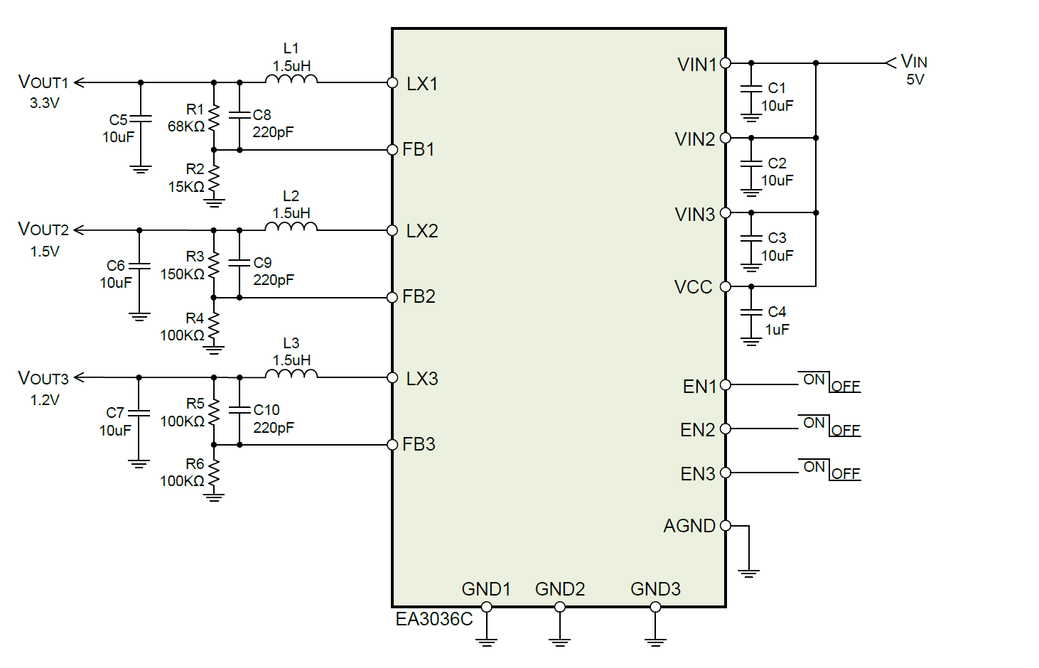
Typical Application Circuit
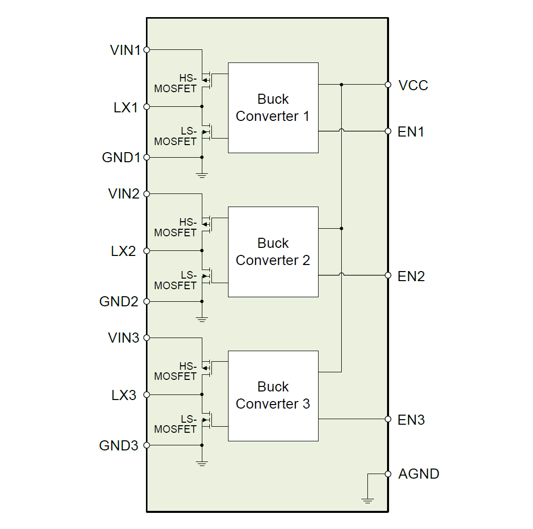
Internal Functional Block Diagram
Pin Definitions
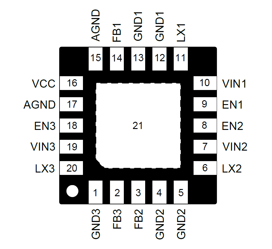
| Pin Name | Pin Description |
|---|---|
| VCC | Power input for internal control circuit |
| VINx | Power input for channel x, with 10uF MLCC capacitor for decoupling |
| LXx | Internal MOS switch output for channel x, can connect to a low-pass filter for more stable voltage output |
| FBx | Feedback pin for channel x, connected to the voltage output through a voltage divider circuit |
| ENx | Enable pin, should not be left floating |
| GNDx | Ground for channel x |
| AGND | Analog ground |
| Bottom Pad | For heat dissipation, must be connected to ground |
Feature Description
PFM/PWM Mode
Each Buck converter can operate in PFM/PWM mode. If the output current is less than 260mA (typical value), the regulator will automatically switch to PFM mode. In PFM mode, the output voltage and ripple are higher than in PWM mode. However, in light-load conditions, PFM is more efficient than PWM.
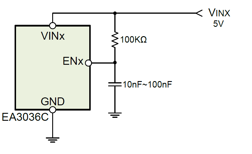
Enable Switching
The EA3036C is a power management IC designed for IPC applications, featuring three 1A synchronous Bucks that can be individually enabled or disabled using the EN pins.
To set the turn-on time for each Buck channel, you can use the circuit shown below:
180° Phase-Shift Architecture
To reduce input ripple current, the EA3036C employs a 180° phase-shift architecture. Buck1 and Buck3 share the same phase, while Buck2 has a phase difference of 180°. This helps to minimize ripple current and consequently reduce EMI.
Overcurrent Protection
Each of the three regulators inside the EA3036C has its own per-cycle current limit circuit. When the peak current in the inductor exceeds the current limit threshold, the output voltage begins to drop until the FB pin voltage falls below the threshold, typically 30% lower than the reference value. Once the threshold is triggered, the switching frequency decreases to 400kHz (typical).
Peak Load Current
The peak load current capability of the EA3036C depends on the internal PMOS current limit, duty cycle (Vout/Vin), and inductance value. Under the conditions of Vin=5V and L=1.5uH, the output peak load current capability is as shown in the following table:
| Output Voltage | Peak Load Current |
|---|---|
| 3.3V | 1.2A |
| 1.8V | 1.5A |
| 1.5V | 1.5A |
| 1.2V | 1.5A |
It is essential to note that the total output power must remain below 6W to prevent chip overheating and damage.
Thermal Shutdown
If the chip's temperature exceeds the thermal shutdown threshold, the EA3036C will automatically shut down. To avoid instability during operation, the hysteresis for thermal shutdown is approximately 30°C.
Output Voltage Adjustment
The output voltage of each regulator can be adjusted using resistor dividers (R1, R2). The output voltage is calculated using the following formula:
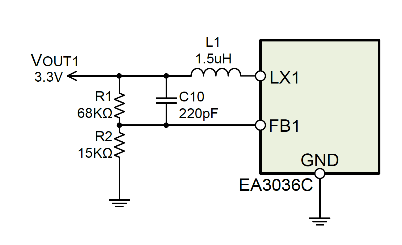
For common output voltage values, you can refer to the table below for resistor divider configurations (using 1% accuracy resistors):
| Output Voltage | R1 | R2 |
|---|---|---|
| 3.3V | 68kΩ | 15kΩ |
| 1.8V | 200kΩ | 100kΩ |
| 1.5V | 150kΩ | 100kΩ |
| 1.2V | 100kΩ | 100kΩ |
Input/Output Capacitor Selection
The input capacitor is used to suppress the noise amplitude of the input voltage, providing stable and clean DC input to the device, while the output capacitor helps to suppress output voltage ripple. Both input and output capacitors can be MLCC capacitors (low ESR).
Recommended models for input/output capacitors are as follows:
| Part Number | Capacitance | Voltage Rating | Package |
|---|---|---|---|
| C2012X5R1A106M | 10uF | 10V | 0805 |
| C3216X5R1A106M | 10uF | 10V | 1206 |
| C2012X5R1A226M | 22uF | 10V | 0805 |
| C3216X5R1A226M | 22uF | 10V | 1206 |
Output Inductor Selection
The choice of the output inductor depends mainly on the ripple current magnitude \(\Delta I_L\) through the inductor. A larger \(\Delta I_L\) results in greater output voltage ripple and losses. While smaller inductors can save cost and space, larger inductance values can yield smaller \(\Delta I_L\), resulting in reduced output voltage ripple and losses. The formula for calculating inductance value is as follows:
For most applications, the EA3036C can use inductors in the range of 1.0~2.2uH.
Power Consumption
The total power consumption of the EA3036C should not exceed 6W, calculated as follows:
Layout Recommendations
A meticulous layout for the PMIC is essential for optimal performance. You can refer to the following suggestions:
- It is advisable to employ a 4-layer PCB layout, with the LX and output planes situated on the top layer, and the VIN plane on an inner layer.
- The ground pins of the top-layer input/output surface mount capacitors should be connected to the inner layer ground and bottom layer ground through vias.
- AGND should be directly connected to the internal ground layer through vias.
- Endeavor to widen traces along high current paths.
- Place input capacitors as close as possible to the VINx pins to minimize noise interference.
- Ensure that the feedback path (from VOUTx to FBx) is positioned away from noise nodes, such as LXx. LXx is a high-current noise node. Use short and wide traces for the layout.
- Multiple vias should be established from the chip's bottom solder pads to the inner layer and bottom layer ground for heat dissipation.
References and Acknowledgments
Original: https://wiki-power.com/ This post is protected by CC BY-NC-SA 4.0 agreement, should be reproduced with attribution.
This post is translated using ChatGPT, please feedback if any omissions.